3D-printed tungsten tiles come through a tokamak plasma campaign at DIII-D
From the Energy digest for Nov 5, 2026
Thread: newgen — 3D-printed tungsten for tokamaks · new
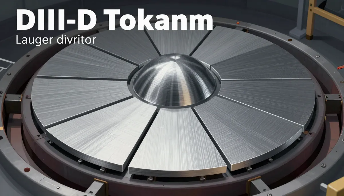
What happened: A team from North Carolina State University, Oak Ridge National Laboratory and JEOL 3D-printed full-size tungsten tiles by electron-beam powder bed fusion and installed flat and domed ones in the DIII-D tokamak's lower divertor in July 2026. Over three days of direct plasma exposure in DIII-D's Tile Testing Campaign, the tiles went through 74 plasma discharges in high-confinement "H-mode" at medium-to-high power; they are now being removed, imaged and surface-scanned for comparison with their pre-exposure condition, with NC State leading the analysis.
What's genuinely new: Full-size plasma-facing components — about 140 by 130 millimetres across, against roughly 50 millimetres for the largest tungsten part NC State had previously printed — produced on JEOL's large-format JAM-5200EBM electron-beam system, with mirror-finish plasma-facing surfaces machined afterward. Earlier button-scale printed-tungsten samples, tested in 2025 on DIII-D's Divertor Materials Evaluation System, saw heat fluxes near 20 MW/m² with brief peaks above 35 MW/m² and showed minimal surface damage. "Most of the field thought printed tungsten would always crack," said ORNL researcher Michael Kirka, whose colleague called the intact tiles additive manufacturing moving "from 'promising' to 'proven' for fusion."
Watch: NC State's post-exposure condition findings, printed tungsten scaled to larger fusion hardware, and pickup by other tokamak programs.
Links: American Nuclear Society · Nov 5, 2:49 PM ET